Objective Lens
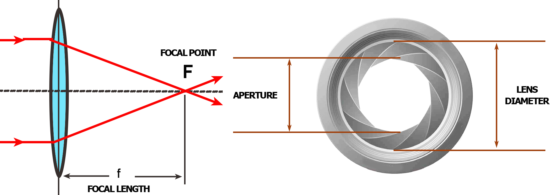
The design of an objective lens and its parameters significantly influence the performance of a thermal imaging device. The focal length of the objective lens directly influences the magnification of the unit (the bigger focal length, the bigger magnification), the field of view (decreases when focal length increases) and detection range.
One can say that the detection range directly depends on the focal length of the objective lens – the bigger focal length, the longer detection range (if the thermal sensor remains the same). The increase of focal length leads to an increase of magnification and a decrease in the field of view.
That is why when designing optical device it is necessary to take into account the tasks that the device has to perform – detect the object at long ranges and identify it due to its high magnification or find object fast due to its wide field of view
.
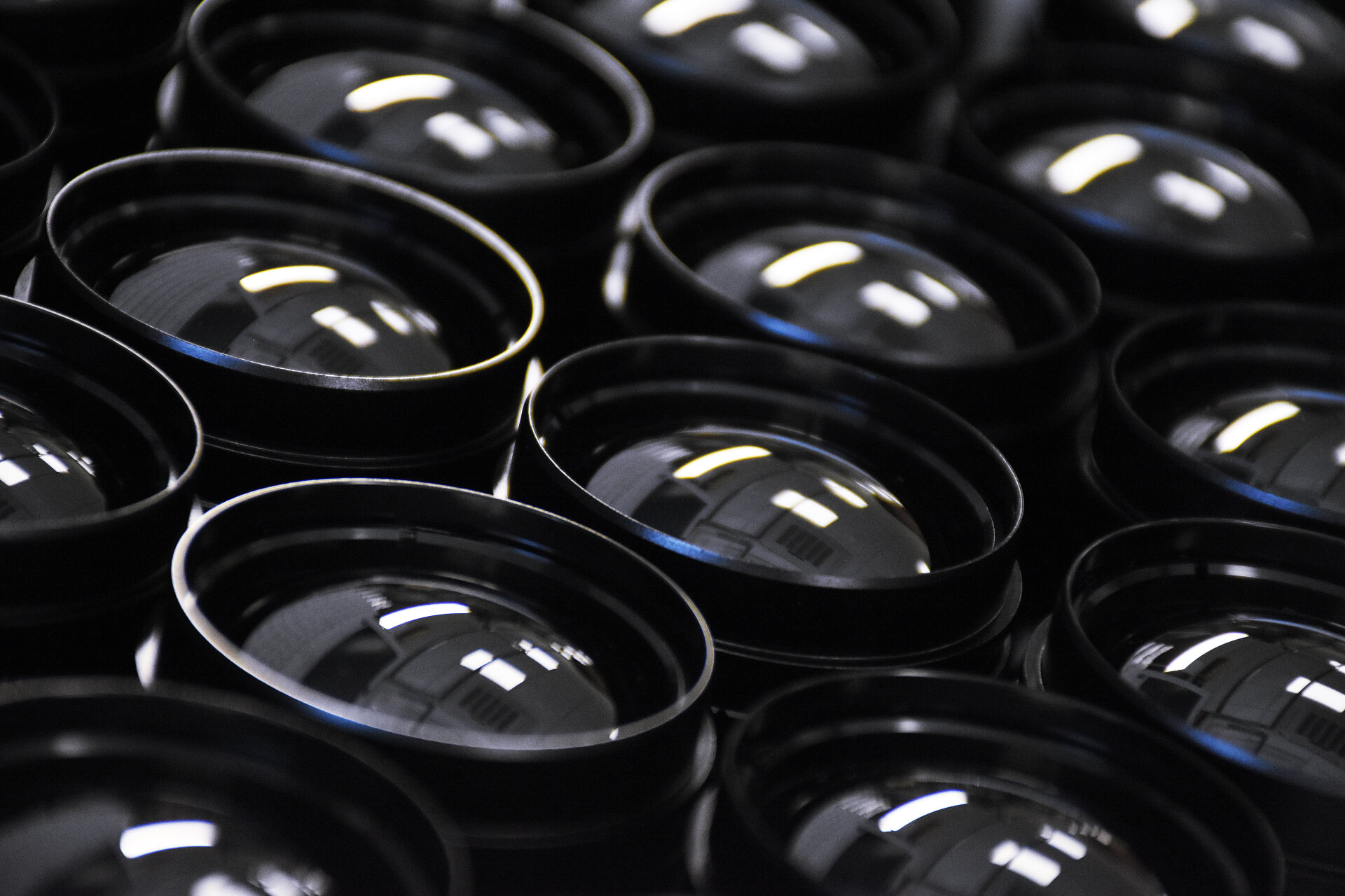
The most widely spread, but not the only, material used for manufacturing objective lenses of thermal imaging devices is single-crystal germanium, chalcogenide glass is also commonly used. To a certain extent sapphire, zinc selenide, silicon and polyethene also possess transmissivity in the MWIR and LWIR ranges.
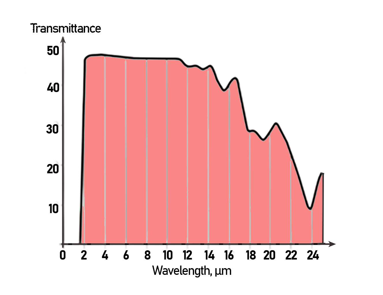
Optic germanium possesses high transmittance and a respectively low absorption coefficient in the range 2 – 15 µm. It is worth mentioning that this range covers two atmospheric transparency windows (3 - 5 and 8 - 12 µm). Most detectors used for civilian and military purposes operate in this range.
Germanium is an expensive material; this is the reason why they strive to make optical systems with a minimal amount of germanium components. Sometimes, to make objective lenses cheaper, mirrors with spherical or aspherical surfaces are applied. For the protection of the lens from external impact, special coatings based on diamond-like carbon (DLC) or similar materials are used.
Classic optical glass is not used for manufacturing objective lenses of thermal imagers because it does not possess transmissivity in the waveband exceeding 4µm.
Relative aperture of objective lens is calculated by taking the lens opening diameter (or pupil diameter) and dividing it by the focal length of the objective lens. It characterizes the amount of energy that can pass through the lens. Relative aperture value influences sensitivity as well as the thermal resolution of a thermal imager.
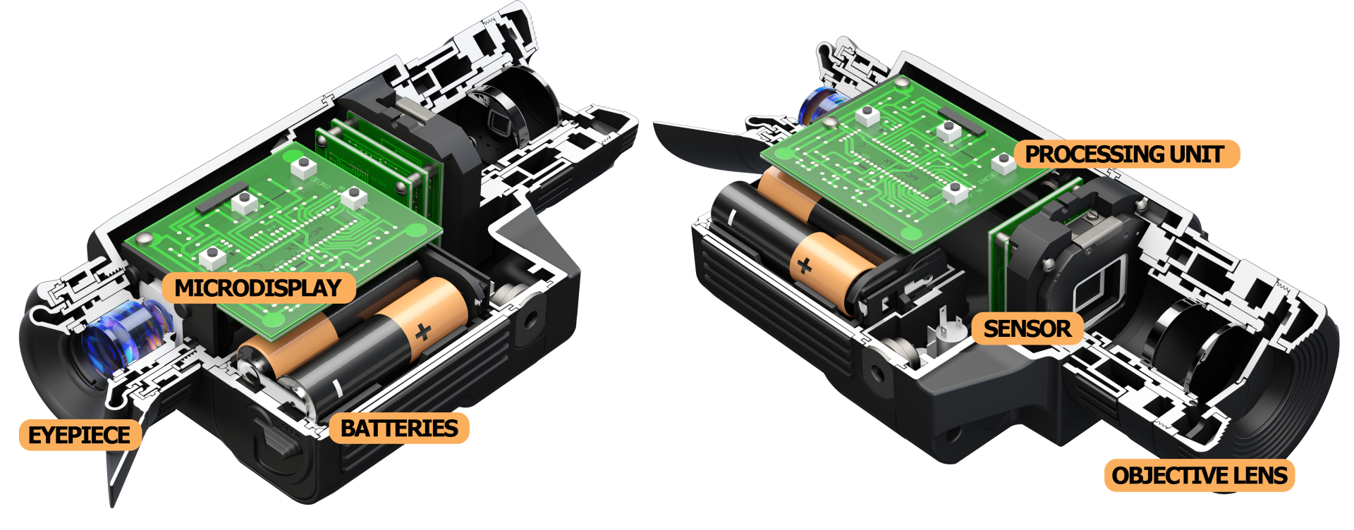
Thermal Sensor (Microbolometer)
The photosensitive element of a thermal imaging unit is a two-dimensional array of photodetectors – the focal plane array (FPA) and is based on various semiconductor materials. There are numerous technologies for manufacturing infrared-sensitive elements, however in the civilian field bolometers (microbolometers) prevail.
The microbolometer is a detector of infrared radiation that registers the change of electrical conductivity of a sensitive element when heated during radiation absorption.
Microbolometers are subdivided into classes depending on what sensitive material is used, this could be vanadium oxide (VOx) or amorphous silicon (α-Si).
The sensitive material absorbs infrared radiation and as a result, according to the law of energy conservation, the sensitive area of a pixel (single photosensitive element) is heated. The internal electric conductivity of an element alters and these changes are registered. The result is a monochrome or colour visualization of temperature image on the display of the unit. It is worth mentioning, that colour palettes on the screen fully depend on the software element of a thermal imaging device.

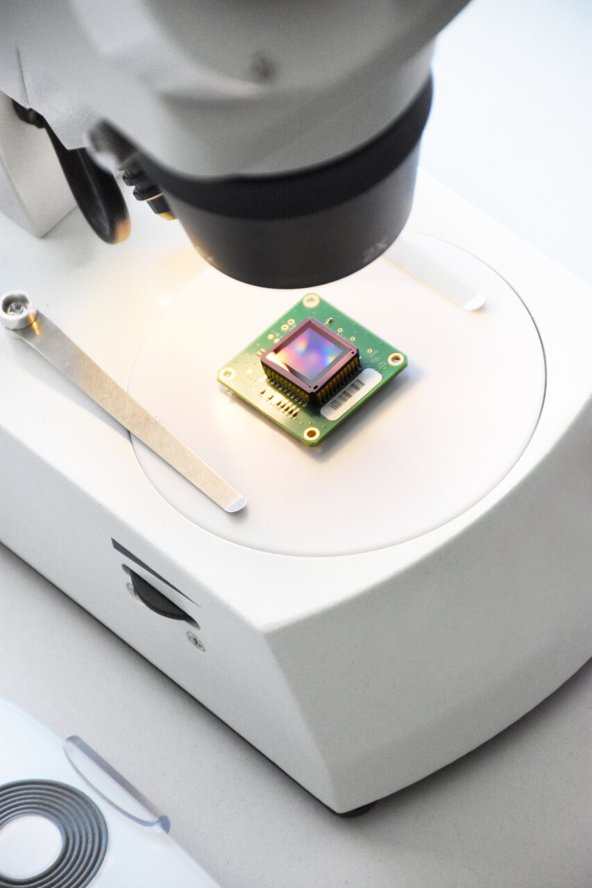
Microbolometer array (sensor) ULIS
Thermal imaging detector (microbolometer) manufacturers produce documents detailing the quality of their sensors. All manufacturers allow for the presence of separate pixels as well as clusters that have deviations of an input signal in the course of normal work – these are known as “dead” or “hot” pixels. “Hot/dead” pixels are present in detectors made by every manufacturer.
Their presence is explained by various deviations that may occur during the microbolometer production as well as by the presence of alien substances in the materials from which microbolometers are produced. When a thermal imager operates the temperature of the pixels increases and pixels that are unable to endure the high temperatures (“Hot”) start producing a signal that differs greatly from those pixels that operate correctly. On the screen of the thermal imager, these pixels can look like white or black dots (in case of single pixels) or spots of varying configuration and size (in case of clusters) or brightness (very bright or very dark). The presence of such pixels does not influence, in any way, the lifetime and operation of the detector and is not the reason for the future deterioration of its parameters, in fact, it can just be considered a “cosmetic” defect.
The manufacturers of thermal imaging detectors apply various algorithms for processing the signal from defective pixels that aim to minimize their influence on image quality and their visibility.
The essence of this processing is in substituting the signal from the defective pixel with the signal of a neighbour (the closest) normally functioning pixel or by an average signal from several neighbouring pixels. As a result of such processing, the defective pixels become practically unnoticeable in the image.
In certain conditions, it is still possible to see the presence of corrected defective pixels (especially clusters), for instance, when a border between hot and cold object is in the field of view, especially when this border gets between a cluster of defective pixels and normal pixels. If both of these conditions coincide the cluster becomes noticeable as a spot displaying white and dark shades and resembling a water droplet in the image. It is worse mentioning that presence of such an effect is not a sign of a defective thermal imaging device.
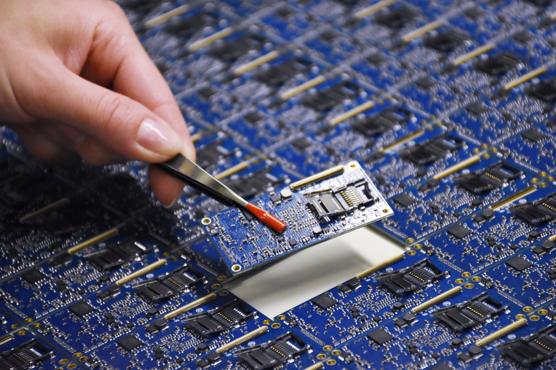
Electronic Processing Unit
The electronic processing unit usually consists of one or several printed circuit boards (depending on the design of the unit), with specialized microcircuits responsible for processing the signal from the sensor and passing it further to display where an image of temperature distribution is formed. The boards also contain main control elements of device and power distribution circuits.
Microdisplay & Eyepiece
Since the majority of hunting thermal imagers use microdisplays, it is necessary to use an eyepiece for image viewing which operates as a magnifying glass and allows to view the magnified image comfortably.
Most commonly used are liquid crystal displays of a transmissive type (where the display is lit up from the reverse side) or OLED displays (when an electric current is applied its substance starts emitting light).
The use of OLED displays has several advantages: the ability to use the device in low temperatures, higher image brightness and image contrast, more simple and reliable design (no backlight source as in LCD). Apart from LCD and OLED displays, LCOS (Liquid Crystal on Silicone) displays can also be used, which are a variety of reflective type LCDs.
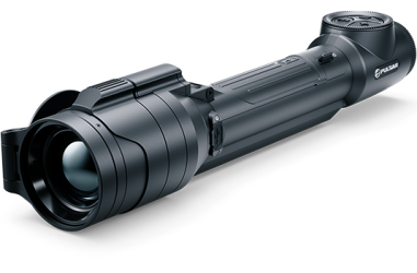
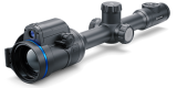
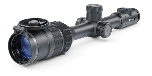
 Thermion 2 LRF XL50
Thermal Imaging Mirini
Thermion 2 LRF XL50
Thermal Imaging Mirini
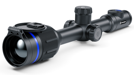
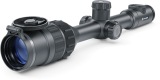
 Thermion 2 LRF
Thermal Imaging Mirini
Thermion 2 LRF
Thermal Imaging Mirini
 Talion
Thermal Imaging Mirini
Talion
Thermal Imaging Mirini
 Thermion 2
Thermal Imaging Mirini
Thermion 2
Thermal Imaging Mirini
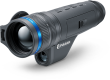
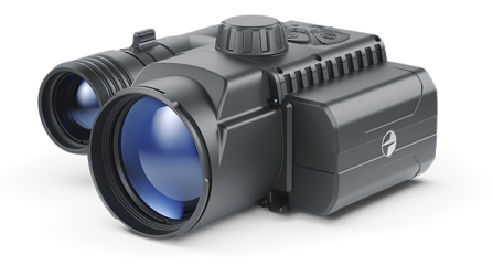
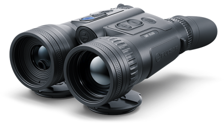 Merger LRF XL50
Binocolo termico
Merger LRF XL50
Binocolo termico
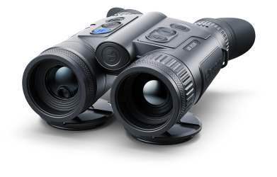
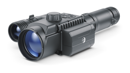
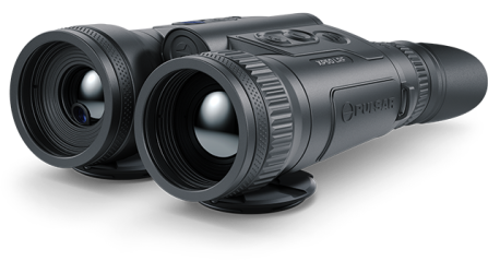 Merger LRF XP50
Binocolo termico
Nuovo
Merger LRF XP50
Binocolo termico
Nuovo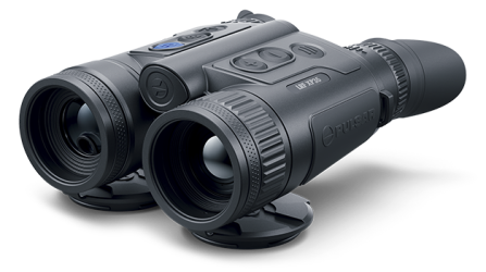 Merger LRF XP35
Binocolo termico
Merger LRF XP35
Binocolo termico
 Merger LRF XQ35
Binocolo termico
Nuovo
Merger LRF XQ35
Binocolo termico
Nuovo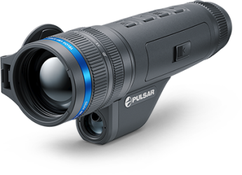 Telos
Ambiti di imaging termico
Telos
Ambiti di imaging termico
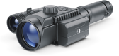
 Axion 2 LRF
Ambiti di imaging termico
Axion 2 LRF
Ambiti di imaging termico
 Axion 2
Ambiti di imaging termico
Nuovo
Axion 2
Ambiti di imaging termico
Nuovo Axion XQ30 PRO
Ambiti di imaging termico
Axion XQ30 PRO
Ambiti di imaging termico
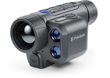
 Krypton 2
Ambiti di imaging termico
Krypton 2
Ambiti di imaging termico
 Axion XM30F
Ambiti di imaging termico
Axion XM30F
Ambiti di imaging termico
 Pulsar Digex-XS
Illuminatori a infrarossi esterni
Pulsar Digex-XS
Illuminatori a infrarossi esterni
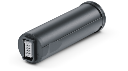 Pacchi Batteria APS
Pacchi Batteria
Pacchi Batteria APS
Pacchi Batteria
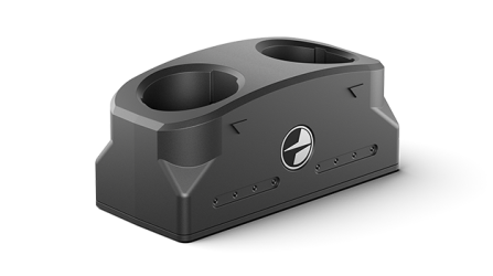 Caricatore di Batterie APS
Caricatore di Batterie
Caricatore di Batterie APS
Caricatore di Batterie
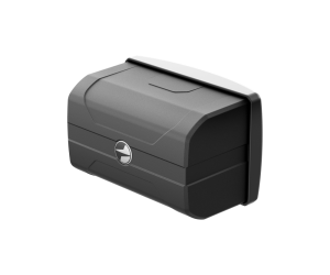 Pacchi Batteria IPS
Pacchi Batteria
Pacchi Batteria IPS
Pacchi Batteria
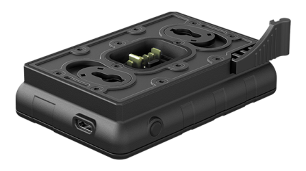 Caricatore di Batterie IPS
Caricatore di Batterie
Caricatore di Batterie IPS
Caricatore di Batterie
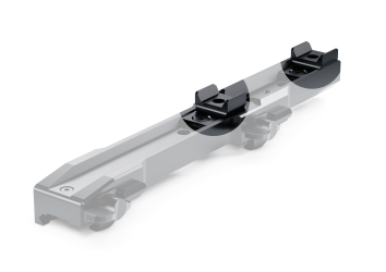
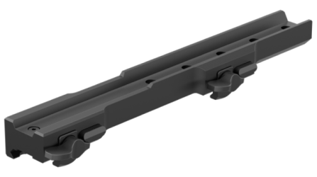 Supporto per Fucile
per Cannocchiali Pulsar
Supporto per Fucile
per Cannocchiali Pulsar
 Distanziatori H7
Kit di riparazione
Nuovo
Distanziatori H7
Kit di riparazione
Nuovo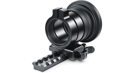 PSP-V Weaver Rail Adapter
Adapter
PSP-V Weaver Rail Adapter
Adapter
 PSP Ring Adapters
Adapters
Nuovo
PSP Ring Adapters
Adapters
Nuovo Adattatori ad anello PSP-B
Adattatori ad anello
Adattatori ad anello PSP-B
Adattatori ad anello
 Adattatori ad Anello della Copertura FN
Adattatori ad Anello della Copertura
Adattatori ad Anello della Copertura FN
Adattatori ad Anello della Copertura
 Telecomandi Wireless
per dispositivi digitali e visori termici
Telecomandi Wireless
per dispositivi digitali e visori termici
 Supporto per morsetto
Accessories Pulsar
Supporto per morsetto
Accessories Pulsar
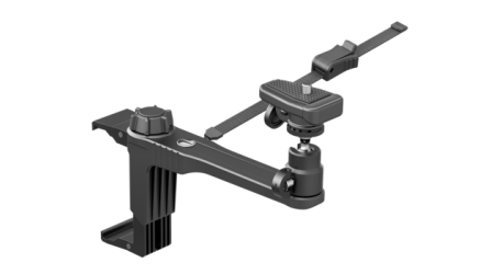
 SUPPORTO PER ALBERI
Accessories Pulsar
SUPPORTO PER ALBERI
Accessories Pulsar
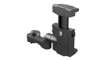
 SUPPORTO PER STRUTTURA FINESTRA
Accessories Pulsar
SUPPORTO PER STRUTTURA FINESTRA
Accessories Pulsar
 Supporto Telefono HELION FLIP-UP
Accessories Pulsar
Supporto Telefono HELION FLIP-UP
Accessories Pulsar
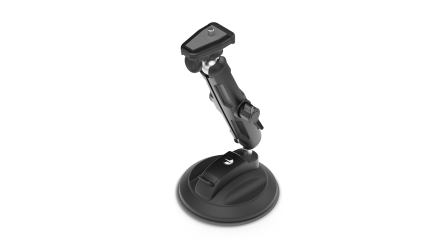 Supporto per vetro liscio
Accessories Pulsar
Supporto per vetro liscio
Accessories Pulsar
 Cinturino
Accessories Pulsar
Nuovo
Cinturino
Accessories Pulsar
Nuovo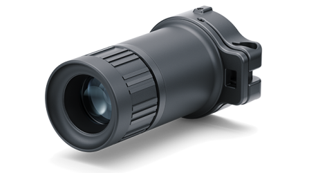 Monocolo Pulsar 3x20 B
Accessori
Monocolo Pulsar 3x20 B
Accessori
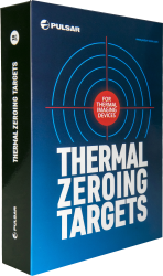 Bersagli per L’azzeramento di Dispositivi Termici
Accessories
Bersagli per L’azzeramento di Dispositivi Termici
Accessories
 Telos LRF Tripod Adapter
Accessories Pulsar
Telos LRF Tripod Adapter
Accessories Pulsar


 English
 German
 French
 Spanish
 Italiano
 English
 Lietuvių